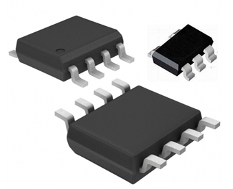
50V/1.5A Step-down High Brightness LED Driver PT4115EE89E
PT4115EE89E GENERAL DESCRIPTION
The PT4115E is a continuous conduction mode inductive step-down converter, designed for driving single or multiple series connected LED efficiently from a voltage source higher than the total LED chain voltage. The device operates from an input supply between 6V and 50V and provides an externally adjustable output current of up to 1.5A. The PT4115E includes the power switch and a high-side output current sensing circuit, which uses an external resistor to set the nominal average output current, and a dedicated DIM input accepts either a DC voltage or a wide range of pulsed dimming. Applying a voltage of 0.3V or lower to the DIM pin turns the output off and switches the device into a low current standby state.
The PT4115EE89E is available in SOT89-5 package.
PT4115EE89E FEATURES
●Simple low parts count
●Wide input voltage range: 6V to 50V
●Up to 1.5A output current
●Single pin on/off and brightness control using DC voltage or PWM
●Typical 3% output current accuracy
●Up to 1MHz switching frequency
●Typical 3% output current accuracy
●Inherent open-circuit LED protection
●High efficiency (up to 97%)
●Inherent Rcs open protection
●High-Side Current Sense
●Hysteretic Control: No need compensation
●Adjustable Constant LED Current
●Thermal shutdown
PT4115EE89E APPLICATION
●Low voltage halogen replacement LEDs
●Automotive lighting
●LED back-up lighting
●Low voltage industrial lighting
●Illuminated signs
●SELV lighting
●LCD TV backlighting
PT4115EE89E ORDERING INFORMATION
PACKAGE
| TEMPERATURE RANGE | ORDERING PART NUMBER | TRANSPORT MEDIA | MARKING
|
SOT89-5
| -40℃ 到85℃ | PT4115EE89E
| Tape and Reel 1000 units |  PT4115E PT4115E
xxxxxX |
PT4115EE89E TYPICAL APPLICATION CIRCUIT

PT4115EE89E PIN ASSIGNMENT

PT4115EE89E OPERATION DESCRIPTION
The PT4115EE89E in conjunction with current sense resistor (RCS),the inductor (L1), and MOSFET forms a self oscillating continuous-mode buck converter.
When input voltage VIN is first applied, the initial current in L1 and RCS is zero and there is no output from the current sense circuit. Under this condition, the output of CS comparator is high. This turns on switch, causing current to flow from VIN to ground, via RCS, the LED(s),L1 and internal MOSFET. The current rises at a rate determined by VIN and L1 to produce a voltage ramp (VCSN) across RCS. When (VIN-VCSN) > 230mV, the output of CS comparator switches low and the switch turns off. The current flowing on the RCS decreases at another rate. When (VIN-VCSN) <170mV, the switch turns on again and the mean current on the LED is determined by 200mV/RCS.
The high-side current-sensing scheme and on-board current-setting circuitry minimize the number of external components while delivering LED current with ±3% accuracy, using a 1% sense resistor. The PT4115EE89E allows dimming with a PWM signal at the DIM input. A logic level below 0.3V at DIM forces PT4115EE89E to turn off the LED and the logic level at DIM must be at least 2.5V to turn on the full LED current. The frequency of PWM dimming ranges from 100Hz to 20 kHz. The DIM pin can be driven by an external DC voltage (VDIM) to adjust the output current to a value below the nominal average value defined by RCS. The DC voltage is valid from 0.5V to 2.5V. When the DC voltage is higher than 2.5V, the output current keeps constant. Additionally, to ensure the reliability, the PT4115EE89E is built with a thermal shutdown (TSD) protection. The TSD protests the IC from over temperature (155℃).
PT4115EE89E APPLICATION NOTES
Setting nominal average output current with external resistor RCS
The nominal average output current is determined by the value of the external current sense resistor (RS) connected between VIN and CSN and is given by: :
IOUT=0.2/Rs
This equation is valid when DIM pin is float or applied with a voltage higher than 2.5V (must be less than 5V). Actually, RCS sets the maximum average current which can be adjusted to a less one by dimming.
Output current adjustment by external DC control voltage
The DIM pin can be driven by an external DC voltage (VDIM), to adjust the output current to a value below the nominal average value defined by RCS.The average output current is given by:

Note that 100% brightness setting corresponds to:(2.5V≤VDIM≤5V)
Output current adjustment by PWM control
A Pulse Width Modulated(PWM) signal with duty cycle PWM can be applied to the DIM pin, to adjust the output current to a value below the nominal average value set by resistor RCS:

PWM dimming provides reduced brightness by modulating the LED’s forward current between 0% and 100%. The LED brightness is controlled by adjusting the relative ratios of the on time to the off time. A 25% brightness level is achieved by turning the LED on at full current for 25% of one cycle. To ensure this switching process between on and off state is invisible by human eyes, the switching frequency must be greater than 100 Hz. Above 100Hz, the human eyes average the on and off times,seeing only an effective brightness that is proportional to the LED’s on-time duty cycle. The advantage of PWM dimming is that the forward current is always constant, therefore the LED color does not vary with brightness as it does with analog dimming. Pulsing the current provides precise brightness control while preserving the color purity. The dimming frequency of PT4115EE89E can be as high as 20kHz.
Soft-start
An external capacitor from the DIM pin to ground will provide additional soft-start delay, by increasing the time taken for the voltage on this pin to rise to the turn-on threshold and by slowing down the rate of rise of the control voltage at the input of the comparator.
Input capacitor selection
A low ESR capacitor should be used for input decoupling, as the ESR of this capacitor appears in series with the supply source impedance and lowers overall efficiency. This capacitor has to supply the relatively high peak current to the coil and smooth the current ripple on the input supply. A minimum value of 10µF is acceptable if the DC input source is close to the device, but higher values will improve performance at lower input voltages, especially when the source impedance is high. The voltage rating should be greater than the input voltage. The input capacitor should be placed as close as possible to the IC. For maximum stability over temperature and voltage, capacitors with X7R, X5R, or better dielectric are recommended. Capacitors with Y5V dielectric are not suitable for decoupling in this application and should not be used.
Inductor selection
Lower value of inductance can result in a higher switching frequency, which causes a larger switching loss. Choose a switch frequency between 100kHz to 500kHz for most application.According to switching frequency, inductor value can be estimated as:

For higher efficiency, choose an inductor with a DC resistance as small as possible.
Output capacitor selection
For most applications,the output capacitor is not necessary. Peak to peak ripple current in the LED(s) can be reduced below 30% of the average current, if required, by adding a capacitor across the LED(s).A value of 2.2µF will meet most requirements. Proportionally lower ripple can be achieved with higher capacitor values. Note that the capacitor will not affect operating frequency or efficiency, but it will increase start-up delay and reduce the frequency of dimming, by reducing the rate of rise of LED voltage.
Thermal considerations
When the device operates at high ambient temperature, or when driving maximum load current, care must be taken to avoid exceeding the package power dissipation limits.
Layout considerations
Pay careful attention to the PCB layout and component placement. RCS should be placed close to the VIN pin and CSN pin in order to minimize current sense error. The input loop including input capacitor,Schottky diode, and MOSFET which should be as short as possible.


