DW8521 2A Peak, 44V Multi-Topology LED Driver
DW8521 General Description
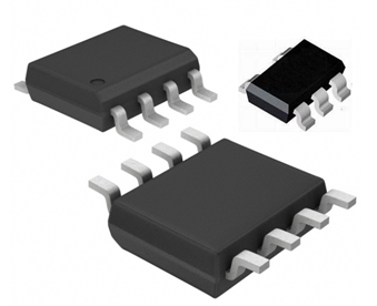
DW8521 is a current mode monolithic LED driver. The LED current can be controlled with an analog input voltage. With high-side LED current sensing, the DW8521 can be configured as buck, boost or buck-boost topology to serve different LED driver need. The integrated 44V/2A N-Channel MOSFETs ensures high efficiency operation. At light loads, DW8521 operates in low frequency to maintain high efficiency and low output ripple. The overvoltage lockout protection on SW pin protects DW8521 from open LED fault. DW8521 also has thermal protection at 140ºC. The DW8521 is available in a 6-pin SOT23-6 and a 8-pin ESOP8 package, which provides a compact solution with minimal external components.
DW8521 Features
- 4.6V to 44V operating input range
- 2A peak switch current
- Analog dimming and PWM dimming
- Constant off-time operation
- SW over voltage lockout
- Thermal protection
- Available in SOT23-6 and ESOP8 package
DW8521 Applications
- LED Driver
DW8521 Pin Information
■DW8521 Pin Placement and IC dimension

■DW8521 Pin Description
SOT23-6L Pin No.. | Pin Name
| Description
|
| 1 | SW
| SW is the switching node. Connect inductor to this pin.
|
| 2 | GND
| Ground pin.
|
| 3 | EN/DIM
| Drive EN/DIM pin above 1.1V to enable the LED driver. To achieve dimming, drive the EN/DIM pin with a PWM pulse or an analog voltage between 1.2V and 2.4V. |
| 4 | ISN
| LED current negative sensing pin. Connect a resistor between ISP and ISN to set full LED current. |
| 5 | ISP
| LED current positive sensing pin.
|
| 6 | VIN
| Input voltage pin. VIN supplies power to the IC.
|
DW8521 Absolute Maximum Ratings(1)
Symbol
| Parameter
| Ratings
|
VIN, EN/DIM, SW
| VIN, EN/DIM, SW Pin Voltage
| -0.3V ~ 48V
|
ISP, ISN
| ISP, ISN Pin Voltage
| -0.3V ~ 48V
|
ISP-ISN
| ISP to ISN Pin Voltage
| -0.3V to 6V
|
θJA
| Package Thermal Resistance(2) | 220 ℃/W
|
θJC | Package Thermal Resistance(2) | 130 ℃/W
|
TJOPR
| Junction Operating temperature
| 40~+125℃
|
TSTG
| Storage Temperature
| -65 ~ 150 ℃
|
TJ | Junction temperature(3),(4) | 150℃
|
Note (1) Stresses above the max. Values listed here may cause permanent damage to the device. Exposure to absolute maximum rating conditions for extended periods may affect device reliability. Maximum ratings are absolute ratings; exceeding only one of these values may cause irreversible damage to the integrated circuit.
(2) θJA is measured in the convection at Ta=30℃ on a high effective thermal conductivity test board(4 Layers, 2S2P) of JEDEC 51-7 thermal measurement standard. PCB dimension is 100x100x1.6mm and 4 layers.
DW8521 Typical Application Circuit

DW8521 2A Peak, 44V Multi-Topology LED Driver Detailed Descriptions
The DW8521 is a current-mode LED driver that can be configured as boost, buck or buck-boost topology.
■Current-Mode Control
The DW8521 operates in constant off-time in heavy load. At light load DW8521 extends the off time to minimize power consumption in the IC.
■DW8521 Dimming
The DW8521 EN/DIM pin serves as analog dimming input. And can also be used for a PWM dimming, where the output crrent is proportional to the duty cycle of the PWM square pulses.
The analog dimming range is 1.2V ~ 2.4V corresponding to the LED current sensing voltage of 0~200mV. Refer to the dimming curve.

■Thermal Protection
DW8521 has thermal protection that shuts down the part at 140℃, and resumes operation after the temperature drops to below 130℃.LED Current Setting The output current is determined by the resistor RSENSE connected between ISP and ISN, and the output current can be calculated by:

For example, for ILED=1A, RFB=200mΩ.
■DW8521 Analog Dimming
Apply a 1.2V~2.4V DC voltage to the EN/DIM pin to control the output current, and the DIM voltage is proportional to the output current.
■DW8521 PWM Dimming
A PWM pulse can also be applied to the EN/ DIM pin to achieve dimming. When PWM dimming, the LED current is proportional to the duty cycle of the PWM square pulse.
■DW8521 Input Capacitor
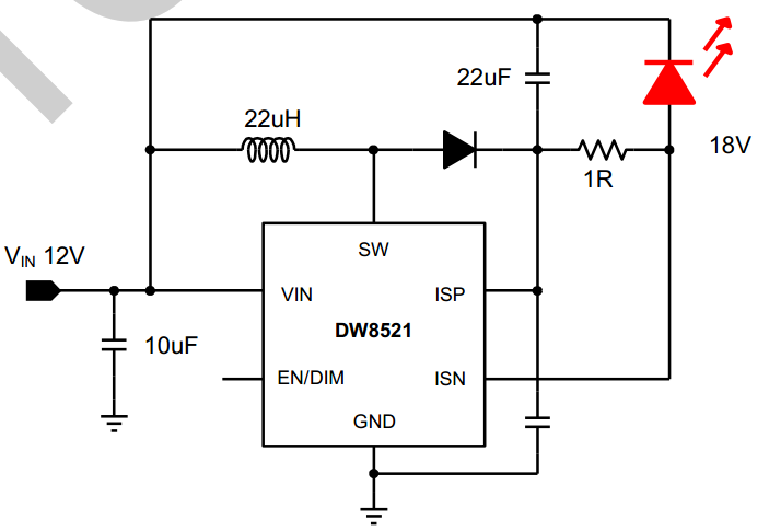
The input capacitor is used to reduce the surge current from the input supply and maintaining the DC input voltage. It can be electrolytic, tantalum or ceramic. To minimizing the switching noise, a small X5R or X7R ceramic capacitor, i.e. 0.1uF, should be placed as close to the IC as possible when using electrolytic capacitors.A 10uF ceramic capacitor is sufficient for most application.
■DW8521 Output Capacitor
The output capacitor is required to maintain the DC output voltage, and the capacitance value determines the output ripple voltage. It can be low ESR electrolytic, tantalum or ceramic, which lower ESR capacitors get lower output ripple voltage. The output capacitors also affect the system stability and transient response, and a 22uF ceramic capacitor is recommended in typical application.
■DW8521 Inductor
The inductor is used to supply constant current to the output load, and the value determines the ripple current which affect the efficiency and the output voltage ripple. The ripple current is typically allowed to be 30% of the maximum switch current limit. DW8521 operates in constant off-time in heavy load, and the inductance can be determined by:

Which toff is the off-time of the MOSFET, ΔI is the inductor ripple current.
After the inductance is determined, the on-time can be calculated by:

Then the frequency also can be calculated by:

Lower DC resistance of the inductor is preferred for higher efficiency.
■DW8521 Start-up Current limit
When using in MR16 application, the output capacitance should be very large to maintain the continuous output current, which causes the failure of the internal soft-start. The following circuit is designed to limit the start-up current.

The ISN voltage is always following the ISP voltage before the output voltage build up, which causes a low feedback voltage and a large start-up current. The resistor R1, R2 and the capacitor C1 are used to slowing down the ISN voltage rising, and the RC time constant should be larger than the startup time.

Where tr is the startup time, and the startup time is about 400us.Because the ISN pin sink current, and to keep the output current sense accuracy, the R1 can bedetermined by :

At steady state, R1 and R2 divide the output voltage, and then, R2 should be larger than R1. In most typical application, R2 can be set to 5 times of R1.
Take all the conditions into consideration, the parameters can be calculated. For example, R1= 300R, R2=2K, and C1=0.1uF.
■DW8521 PCB Layout Precaution
The PCB layout of DW8521 must be carefully designed. Different PCB layout optimization is required for different topology application of DW8521.
1. Place the input decoupling capacitor as close to DW8521 (VIN pin and PGND) as possible to eliminate noise at the input pin. The loop area formed by input capacitor and GND must be minimized.
2. Put the feedback trace as far away from the inductor and noisy power traces as possible.
3. The ground plan on the PCB should be as large as possible for better heat dissipation.
DW8521 Typical Application Circuit
■Step-up LED Driver Application DW8521:

■Step-down LED Driver Application DW8521:

■Step-up/down LED Driver Application DW8521:
