 MS31703NA_Datasheet_En.pdf
Overview of Single Channel H-bridge Gate Driver MS31703NA
The MS31703NA is a small single-channel H-bridge gate driver, which uses four external N-channelMOSFET to drive a bidirectional brushed DC motor.PH/EN, independent H-bridge or PWM are allowed to be connected to the controller circuit easily. The internal sense amplifier can provide adjustable current control. And the integrated charge pumps can provide 100% duty cycle as well as driving external reverse battery switch.
The independent H-bridge mode supports H-bridge sharing and controls several DC motors. The MS31703NA has the built-in circuit, which uses the PWM current chopping with fixed off-time to adjust winding current.
The MS31703NA can reduce electromagnetic interference (EMI) by the programmable slew rate control technology. It can also be applied flexibly and prevent any gate short-circuit issues.
Main features of single channel H-bridge gate driver MS31703NA
◼Single-channel H-bridge Gate Driver
-Drive Four External N-channel MOSFET
-Support 100% Pulse Width Modulation (PWM)Duty Cycle
◼Power Supply Range: 5.5V to 45V
◼Three Control Modes:
-PH/EN, Independent H-bridge and PWM
◼Serial Interface for Configuration
◼Adjustable Slew Rate Control
◼Independent Control of Each H-bridge
◼Support 1.8V, 3.3V and 5V Logic Inputs
◼Current-shunt Amplifier
◼Integrated PWM Current Regulation
◼Low Power Dissipation Sleep Mode
◼Protection Characteristics
-Supply Undervoltage Lockout (UVLO)
-Charge-pump Undervoltage (CPUV) Lockout
-Overcurrent Protection (OCP)
-Gate Drive Fault (GDF)
-Thermal Shutdown (TSD)
-Watchdog Timer
-Fault Regulation Output(nFAULT)
Ruimeng Technology - Single Channel H-bridge Gate Driver MS31703NA Order Information
Part Number
| Marking
| Package
| Package type
|
MS31703NA
| MS31703NA | QFN32
| 1000PCS/Roll
|
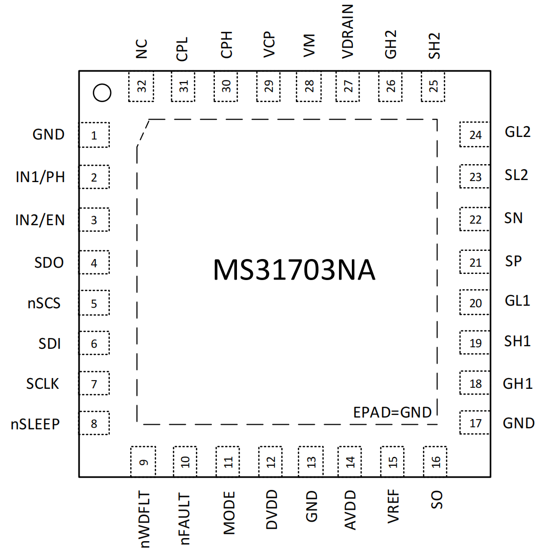
Relmon -Single Channel H-bridge Gate Driver MS31703NA Chip Pin Definition and Packaging Dimensions:

PIN | MS31703NA Name | Type | Function description of 703NA pin driven by single channel H-bridge gate |
1 | GND | - | Ground. |
2 | IN1/PH | I | Input Control Pin. The logic of this pin depends on the MODE pin.This pin is connected to the ground with the internal pull-down resistor. |
3 | IN2/EN | I | Input Control Pin. The logic of this pin depends on the MODE pin.This pin is connected to the ground with the internal pull-down resistor. |
4 | SDO | O | SPI Data Output. This pin is open-drain output, which needs the external pull-up resistor. |
5 | nSCS | I | SPI Select Input. When this pin is pulled low, data input is enabled. |
6 | SDI | I | SPI Data Input. This pin is connected to the ground with the internal pull-down resistor. |
7 | SCLK | I | SPI Clock Input. This pin is connected to the ground with the internal pull-down resistor. |
8 | nSLEEP | I | Sleep Mode Input Pin. Pull this pin to logic low to make the device in low power dissipation sleep mode with the FET in high-impedance state (Hi�Z). This pin is connected to the ground with the internal pull-down resistor. |
9 | nWDFLT | O | Watchdog Fault Indication Pin. When the watchdog fault occurs, this pin is pulled low. This pin is open-drain output, which needs the external pull-up resistor. |
10 | nFAULT | O | Fault Indication Pin. When the fault occurs, this pin is pulled low. This pin is open-drain output, which needs the external pull-up resistor. |
11 | MODE | I | Mode Control Pin. When this pin is pulled to logic low, enabling EN/PHcontrol mode. When this pin is pulled to logic high, enabling independent H-bridge mode. When this pin is hanging, enabling PWMcontrol mode. When this pin is powered on or exits sleep mode, operation of this pin is latched. This pin is connected to the internal pull�up and pull-down resistors. |
12 | DVDD | O | 3.3V Logic Power Supply Output. This pin is connected to the ground with a 1µF bypass capacitor. |
13 | GND | - | Ground. |
14 | AVDD | O | 5V Analog Power Supply Output. This pin is connected to the groundwith a 1µF bypass capacitor. |
15 | VREF | I | Analog Reference Voltage Input. This pin controls chopping current. |
16 | SO | O | Shunt Amplifier Output. The capacitor on this pin can not exceed 1nF. |
17 | GND | - | Ground |
18 | GH1 | I | High-side Gate. Connect this pin to high-side FET gate. |
19 | SH1 | I | High-side Source. Connect this pin to high-side FET source. |
20 | GL1 | O | Low-side Gate. Connect this pin to low-side FET gate. |
21 | SP | I | Shunt Amplifier Positive Input. Connected to positive terminal of senseresistor. |
22 | SN | I | Shunt Amplifier Negative Input. Connected to negative terminal of senseresistor. |
23 | SL2 | I | Low-side Source. Connect this pin to low-side FET source. |
24 | GL2 | O | Low-side Gate. Connect this pin to low-side FET gate. |
25 | SH2 | I | High-side Source. Connect this pin to high-side FET source. |
26 | GH2 | O | High-side Gate. Connect this pin to high-side FET gate. |
27 | VDRAIN | I | High-side Drain. Connect this pin to high-side FET drain. |
28 | VM | - | Power Supply. Connect this pin to the motor power supply. This pin is connected to the ground with a 0.1µF and the minimum 10µF bypass capacitors. |
29 | VCP | I/O | Charge-pump Voltage. Connected to VM with a 1µF capacitor. |
30 | CPH | I/O | Charge-pump Capacitor Output. |
31 | CPL | I/O | Charge-pump Capacitor Input. Connected to CPH with a 0.1µF capacitor. |
32 | NC | - | Not Connection. |
Internal circuit BLOCK DIAGRAM of single channel H-bridge gate driver MS31703NA

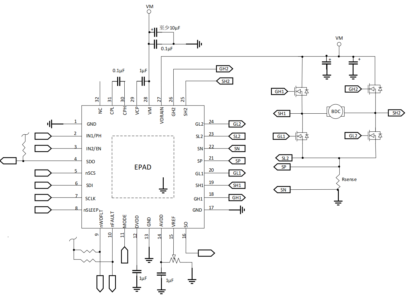
Ruimeng Technology - Single Channel H-bridge Gate Driver MS31703NA Chip Typical Application Circuit

Ruimeng Technology - Single Channel H-bridge Gate Driver MS31703NA Chip Function Description
The MS31703NA controls four external NMOSFETs to drive bidirectional brushed DC motors. TheMS31703NA can also operate in independent H-bridge mode to drive two directional brushed DC motors. It supports power supply from 5.5V to 45V and enables low power dissipation sleep mode through the nSLEEP pin. The control mode has three options, including configurable PH/EN, independent H-bridge control or PWM mode, which is easy to be connected with controller circuit.
The MS31703NA can adjust gate drive strength or gate drive current to optimize different FET applications without external resistors. The device number of motor drive systems are strikingly reduced by integrating the needed FET drive circuits into the single device. The peak current can be adjusted through SPI. When VM voltage is more than 13.5V, high-side and low-side FETs are driven with 10.5V (nominal) gate source voltage (VGS). At lower VM voltage, the VGS is reduced. The high-side gate drive voltage is generated through a double-structure charge-pump that regulated to VM+10.5V.
The shunt amplifier gain of the MS31703NA can be configured through SPI. The current can be limited by the current chopping way with internal fixed off-time.
The MS31703NA has complete protection functions, including: undervoltage lockout(UVLO), overcurrent protection(OCP), gate drive faults and thermal shutdown(TSD).
The MS31703NA integrates the spread spectrum clock function of internal digital oscillator and charge pumps, which is combined with output conversion rate to minimize radiation.


