


APM Primary Agent 12–250V Trench N-MOSFET AP8N06SI
- Model:
- AP8N06SI
- Brand:
- APM
- Batch No:
- AP8N06SI,AP8N06SI MOS 管,60V 8.5A 场效应管,SOT89-3L N 沟道 MOS, 低内阻锂电池保护开关,4.5V 低压驱动 MOS, 永源微 MOSFET, 国产替代
- Desc:
- Buy original APM AP8N06SI N-channel MOSFET (60V 8.5A SOT89-3L). Typical 28mΩ Rds(on), 4.5V low gate drive, high avalanche energy. GSMICRO authorized distributor with free samples, replaces AO6606 & HC070N06LS for power tools, power banks and DC-DC modules
- Stock:
- 15000 PCS
AP8N06SI 60V/8.5A N-Channel Enhancement Mode MOSFET SOT89-3L SMD
SEO Keywords: AP8N06SI, AP8N06SI MOSFET, 60V 8.5A N Channel MOS, SOT89-3L Field Effect Transistor, Low Rds(on) MOSFET, Battery Protection MOS, Load Switch MOS, APM AP8N06SI, Domestic Replacement MOS
Product Core Parameter Summary: AP8N06SI is an N-channel enhancement mode MOSFET manufactured by APM Microelectronics with SOT89-3L package. Adopting advanced trench technology, VDS breakdown voltage reaches 60V, continuous drain current up to 8.5A at 25℃. Typical Rds(on) is only 28mΩ under VGS=10V, supports 4.5V minimum gate drive voltage compatible with 3.3V MCU IO. Low total gate charge delivers fast switching speed, single pulse avalanche energy 21.5mJ. Operating temperature ranges from -55℃ to 150℃ with max power dissipation 1.2W. Integrated body freewheeling diode inside. Widely applied in lithium battery protection boards, DC-DC converters and load switches. GSMICRO keeps original stock and can directly replace AO6606, HC070N06LS and other domestic & imported MOS parts with the same package.
AP8N06SI MOS Product Overview
AP8N06SI is an N-channel enhancement power MOSFET launched by APM Microelectronics. Built with advanced trench semiconductor technology, it features ultra-low on-resistance and low gate charge. It can be driven at gate voltage as low as 4.5V without extra boost circuit for MCU direct control. Packaged in compact SOT89-3L SMD with excellent heat dissipation performance. Rated VDS 60V and continuous drain current 8.5A, single pulse avalanche energy 21.5mJ. Operating temperature: -55℃ ~ 150℃, fully RoHS compliant. Mainly used for battery protection, load switch and small uninterruptible power supply power switching circuits.
GSMICRO is an authorized first-tier distributor of APM Microelectronics. We provide AP8N06SI full reel stock, free samples, complete datasheets, standard application circuits and PCB layout guidance with tiered volume quotation service.
Core Advantages of AP8N06SI
1. Advanced trench process with ultra-low Rds(on), typical 28mΩ @ VGS=10V, low heating under full load and higher system conversion efficiency;
2. Supports 4.5V low gate drive, directly driven by 3.3V/5V MCU IO without boost circuits to simplify BOM list;
3. Low total gate charge Qg=20.3nC, fast turn-on & turn-off speed with minor switching loss, suitable for high-frequency switching circuits;
4. 60V high breakdown voltage, max continuous ID 8.5A, peak pulse IDM 14.6A, single pulse avalanche energy 21.5mJ with strong surge resistance;
5. Integrated body diode with maximum forward current 20A, ideal for bidirectional load and anti-reverse protection circuits;
6. Mini SOT89-3L SMD package, small PCB footprint for portable digital & battery-powered devices;
7. Stable electrical performance from -55℃ to 150℃, reliable for outdoor and vehicle electronics;
8. Factory standard tape & reel packing (3000pcs/reel) for fully automatic SMT production, GSMICRO stable stock & short lead time;
Complete Electrical Specifications
Absolute Maximum Ratings (TC=25℃)
| Parameter Name | Symbol | Rating | Unit |
| Drain-Source Voltage | VDS | 60 | V |
| Gate-Source Voltage | VGS | ±20 | V |
| Continuous Drain Current @25℃ | ID | 8.5 | A |
| Continuous Drain Current @70℃ | ID | 5.8 | A |
| Pulsed Drain Current | IDM | 14.6 | A |
| Single Pulse Avalanche Energy | EAS | 21.5 | mJ |
| Avalanche Current | IAS | 20.6 | A |
| Total Power Dissipation @25℃ | PD | 1.2 | W |
| Storage Temperature Range | TSTG | -55~150 | ℃ |
| Operating Junction Temperature | TJ | -55~150 | ℃ |
| Thermal Resistance Junction to Ambient | RθJA | 62.5 | ℃/W |
| Thermal Resistance Junction to Case | RθJC | 36 | ℃/W |
Electrical Characteristics (TJ=25℃)
| Parameter | Test Condition | Min | Typ | Max | Unit |
| Drain-Source Breakdown Voltage V(BR)DSS | VGS=0V,ID=250μA | 60 | 65 | - | V |
| Zero Gate Drain Current IDSS | VDS=60V,VGS=0V | - | - | 1.0 | μA |
| Gate Leakage Current IGSS | VDS=0V,VGS=±20V | - | - | ±100 | nA |
| Gate Threshold Voltage VGS(th) | VDS=VGS,ID=250μA | 1.0 | 1.6 | 2.5 | V |
| Static On-Resistance RDS(on) | VGS=10V,ID=10A | - | 28 | 40 | mΩ |
| Static On-Resistance RDS(on) | VGS=4.5V,ID=5A | - | 33 | 45 | mΩ |
| Input Capacitance Ciss | VDS=25V,f=1MHz | - | 1148 | - | pF |
| Output Capacitance Coss | VDS=25V,f=1MHz | - | 58.5 | - | pF |
| Reverse Transfer Capacitance Crss | VDS=25V,f=1MHz | - | 49.4 | - | pF |
| Total Gate Charge Qg | VDS=30V,ID=10A | - | 20.3 | - | nC |
| Turn-on Delay td(on) | VDS=30V,RG=1.8Ω | - | 7.6 | - | ns |
| Rise Time tr | VDS=30V,RG=1.8Ω | - | 20 | - | ns |
| Turn-off Delay td(off) | VDS=30V,RG=1.8Ω | - | 15 | - | ns |
| Fall Time tf | VDS=30V,RG=1.8Ω | - | 24 | - | ns |
| Body Diode Forward Voltage VSD | IS=20A | - | - | 1.2 | V |
| Body Diode Reverse Recovery Time trr | IF=20A,dI/dt=100A/μs | - | 29 | - | ns |
Pinout, Internal Circuit & Package Dimension
SOT89-3L Pin Definition
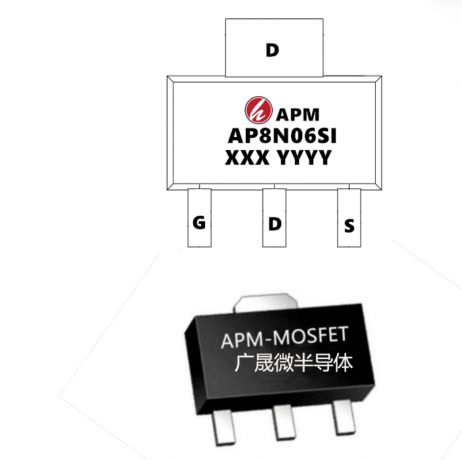
AP8N06SI adopts standard SOT89-3L 3-pin SMD layout: Pin1=Gate(G), Pin2=Drain(D), Pin3=Source(S). Bottom metal pad connected to Drain terminal. Large copper area on PCB can lower thermal rise and boost continuous current capacity. The chip integrates N-channel MOS and parallel freewheeling body diode, supporting bidirectional current flow to simplify anti-reverse load circuits.
Internal Circuit Diagram Description
Vertical trench MOS structure with ±20V gate-source isolation voltage and 60V drain-source blocking voltage. Body diode connected between D & S for inductive load freewheeling. Low gate capacitance reduces switching loss, 4.5V low gate input works with general MCU IO without level shift chips.
SOT89-3L Mechanical Dimensions
| Dimension Mark | Min(mm) | Typ(mm) | Max(mm) |
| Pin Width b | 0.40 | - | 0.58 |
| Device Body Width D | 4.40 | 4.50 | 4.60 |
| Thermal Pad D1 | 3.00 | - | 3.30 |
| Pin Length L | 0.90 | - | 1.10 |
Standard SOT89 PCB footprint library is fully compatible with AP8N06SI. Designers should lay large copper area under D pin thermal pad to cut thermal resistance and guarantee stable 8.5A long-time operation.
Typical Application Circuits & Usage Guide
Standard Li-ion Battery Protection Circuit
AP8N06SI is series-connected on battery negative rail, controlled by MCU/protection IC gate pin. High-level signal turns on the discharge channel. Internal body diode enables reverse charging loop. 60V breakdown fits multi-cell lithium packs, 12V/24V portable energy storage equipment.
General Load Switch Circuit
VIN connects to Drain, load to Source. 1k~10k pull-down resistor on MCU IO to Gate. High IO level turns MOS ON, low level cuts off power. Works for LED drivers, small motors, Bluetooth/WiFi module power supply, no booster circuit needed for 3.3V MCU.
Application Notes
1. PCB Thermal Design: Maximize copper area on D pad, derate ID to 5.8A when ambient temperature hits 70℃;
2. Gate Protection: Add 1k~10k series gate resistor to avoid ESD breakdown, pull-down resistor prevents false turn-on;
3. Inductive Load: Add RC snubber circuit across load to suppress inductive voltage spike;
4. Reflow Profile: Lead-free solder peak temp ≤260℃, total high-temp duration ≤40s, seal moisture-proof bag before opening;
Application Fields
1. Li-polymer battery protection: Power bank, cordless vacuum, power tool, portable energy storage power switch;
2. General load switch: LED modules, small DC motors, wireless communication module power control;
3. Mini UPS, DC-DC Buck & Boost Converter Circuits;
4. Consumer Electronics: Bluetooth earbuds, portable fans, beauty instruments, atomizer power control;
5. Smart Home & Security Low-Voltage Switch Circuits;
Ordering & Packaging Info
| Part Number | Package | Marking Code | Quantity Per Reel | Pack Spec |
| AP8N06SI | SOT89-3L | AP8N06SI | 3000pcs | 13-inch Moisture-Proof Tape & Reel |
Factory packed with moisture-proof aluminum foil bags, bulk cart shipment available. GSMICRO supports reel splitting and sample separation, mass order lead time: 3~5 working days.
Cross Reference & Competitive Comparison
Direct Compatible Replacement Parts
Same brand alternative: AP4N06SI (4.8A low-current version);
Domestic equivalent: HC070N06LS, 8N06 SOT89 series;
Import equivalent: ZXMS6005DN8, AO6606, SMF0608;
AP8N06SI VS Competitor Parameter Table
| Comparison Item | AP8N06SI | AO6606 | HC070N06LS |
| VDS Breakdown Voltage | 60V | 60V | 60V |
| Max Continuous ID | 8.5A | 6A | 6A |
| Rds(on) @VGS=10V (Typ) | 28mΩ | 45mΩ | 200mΩ |
| Min Operating VGS | 4.5V | 4.8V | 5V+ |
| Single Pulse EAS | 21.5mJ | 12mJ | 8mJ |
| Package | SOT89-3L | SOT-23 | SOT89 |
| Supply Status | GSMICRO In Stock | Long Import Lead Time | Fluctuating Stock |
AP8N06SI Competitive Strengths
1. Highest 8.5A rated current among SOT89 packages, no need to upgrade large-size package for high-power loads;
2. Much lower on-resistance than domestic competitors, lower device temperature rise and longer battery cycle life;
3. 4.5V low gate drive compatible with 3.3V MCU, eliminate level shift components and cut BOM cost;
4. High single pulse avalanche energy, better resistance against battery short-circuit & inductive spike, lower product failure rate;
5. APM authorized original stock, stable delivery within 3-5 days, lower cost than imported MOS with full technical document support;
Technical Support & Service
1. Free Sample Application: 5~20pcs samples available for prototype testing per customer;
2. Full Technical Documents: Original datasheet, schematic reference, PCB footprint, reflow parameter sheet;
3. Circuit Optimization Support: Battery protection circuit revision, EMC improvement guidance;
4. One-stop BOM Supply: MCU, protection IC, diode, resistor & capacitor full set matching service;
GSMICRO is authorized first-tier distributor of APM Microelectronics. We keep full reel AP8N06SI inventory, provide free samples, datasheets, application schematics, PCB layout service and tiered volume quotation for customers worldwide.
About GSMICRO Semiconductor (Shenzhen) Co., Ltd.
GSMICRO Semiconductor (Shenzhen) Co., Ltd. (Short: GSMICRO) was founded in 2023, while its predecessor LUMENCHIP was established back in 2010. Headquartered in Shenzhen, China, we are a leading integrated analog chip service provider focusing on mixed-signal chip technical implementation and green intelligent electronics development.
GSMICRO integrates global supply chain resources and abandons traditional separate distribution model. We built an all-in-one service platform combining distribution, market forecasting, technical scheme development and one-stop component supply. Our business covers brand agency, self-owned chip products and full-set supporting materials, forming a complementary operation system. Our core mission is to deliver customized innovative products and global supply solutions, helping clients maximize profit and long-term business growth. We communicate in-depth with customers to provide exclusive hardware design suggestions and cost-effective chip solutions, covering MCU, power management, AI voice and signal chain chips for all consumer & industrial electronics segments.
GSMICRO owns a complete product portfolio including MCU, power IC, AI speech chip, signal amplifier & power MOS devices. Authorized global partners include DONGWOON, CR MICRO, CRHJ, APM, COOLSEMI, ANHI, Reasunos, OCX, MassChip, XLSEMI, Hichips, NSIWAY, EGmicro, Ruimeng, ChipWays, AISPEECH, Aerosemi and more brands.
GSMICRO adheres to the core value "Take Strugglers As Foundation, Take Customers As Center, Stick To Value Contribution". We focus on chip technical landing and green semiconductor innovation, ranking top-tier in power device agency and hardware solution industry worldwide. Official Website: https://www.gs-micro.com
- Grade And Comment
- Question And Answer